
Quantum Computing Breakthrough: Photons That Make Quantum Bits “Fly”
Researchers have pioneered a photon-based qubit communication model, facilitating precise control in quantum computing information transfer. Credit: SciTechDaily.comTwo physicists at the University of Konstanz are developing a method that could enable the stable exchange of information in quantum computers. In the leading role: photons that make quantum bits “fly.”Quantum computers are considered the next big evolutionary step in information technology. They are expected to solve computing problems that today’s computers simply cannot solve – or would take ages to do so. Research groups around the world are working on making the quantum computer a reality. This is anything but easy, because the basic components of such a computer, the quantum bits or qubits, are extremely fragile.One type of qubit consists of the intrinsic angular momentum (spin) of a single electron, i.e. they are at the scale of an atom. It is hard enough to keep such a fragile system intact. It is even more difficult to interconnect two or more of these qubits. So how can a stable exchange of information between qubits be achieved? Flying QubitsThe two Konstanz physicists Benedikt Tissot and Guido Burkard have now developed a theoretical model of how the information exchange between qubits could succeed by using photons as a “means of transport” for quantum information.The general idea: The information content (electron spin state) of the material qubit is converted into a “flying qubit,” namely a photon. Photons are “light quanta” that constitute the basic building blocks making up the electromagnetic radiation field.The special feature of the new model: stimulated Raman emissions are used for converting the qubit into a photon. This procedure allows more control over the photons.“We are proposing a paradigm shift from optimizing the control during the generation of the photon to directly optimizing the temporal shape of the light pulse in the flying qubit,” explains Guido Burkard.Illustration of a quantum system (silver arrow and yellow, green and purple orbitals) interacting with a resonator (two mirrors and pink light field between them). In addition, the quantum system is controlled by a control field (green laser). A photon (pink luminous drop) has been emitted into an optical fibre through one of the mirrors. Credit & Copyright: Benedikt TissotBenedikt Tissot compares the basic procedure with the Internet: “In a classic computer, we have our bits, which are encoded on a chip in the form of electrons. If we want to send information over long distances, the information content of the bits is converted into a light signal that is transmitted through optical fibers.”The principle of information exchange between qubits in a quantum computer is very similar: “Here, too, we have to convert the information into states that can be easily transmitted – and photons are ideal for this,” explains Tissot.A Three-Level System for Controlling the Photon“We need to consider several aspects,” says Tissot: “We want to control the direction in which the information flows – as well as when, how quickly, and where it flows to. That’s why we need a system that allows for a high level of control.”The researchers’ method makes this control possible by means of resonator-enhanced, stimulated Raman emissions. Behind this term is a three-level system, which leads to a multi-stage procedure. These stages offer the physicists control over the photon that is created. “We have ‘more buttons’ here that we can operate to control the photon,” Tissot illustrates.Stimulated Raman emission are an established method in physics. However, using them to send qubit states directly is unusual. The new method might make it possible to balance the consequences of environmental perturbations and unwanted side effects of rapid changes in the temporal shape of the light pulse, so that information transport can be implemented more accurately.The detailed procedure was published in the journal Physical Review Research in February 2024.Reference: “Efficient high-fidelity flying qubit shaping” by Benedikt Tissot and Guido Burkard, 8 February 2024, Physical Review Research.DOI: 10.1103/PhysRevResearch.6.013150
Two physicists at the University of Konstanz are developing a method that could enable the stable exchange of information in quantum computers. In the leading...

Researchers have pioneered a photon-based qubit communication model, facilitating precise control in quantum computing information transfer. Credit: SciTechDaily.com
Two physicists at the University of Konstanz are developing a method that could enable the stable exchange of information in quantum computers. In the leading role: photons that make quantum bits “fly.”
Quantum computers are considered the next big evolutionary step in information technology. They are expected to solve computing problems that today’s computers simply cannot solve – or would take ages to do so. Research groups around the world are working on making the quantum computer a reality. This is anything but easy, because the basic components of such a computer, the quantum bits or qubits, are extremely fragile.
One type of qubit consists of the intrinsic angular momentum (spin) of a single electron, i.e. they are at the scale of an atom. It is hard enough to keep such a fragile system intact. It is even more difficult to interconnect two or more of these qubits. So how can a stable exchange of information between qubits be achieved?
Flying Qubits
The two Konstanz physicists Benedikt Tissot and Guido Burkard have now developed a theoretical model of how the information exchange between qubits could succeed by using photons as a “means of transport” for quantum information.
The general idea: The information content (electron spin state) of the material qubit is converted into a “flying qubit,” namely a photon. Photons are “light quanta” that constitute the basic building blocks making up the electromagnetic radiation field.
The special feature of the new model: stimulated Raman emissions are used for converting the qubit into a photon. This procedure allows more control over the photons.
“We are proposing a paradigm shift from optimizing the control during the generation of the photon to directly optimizing the temporal shape of the light pulse in the flying qubit,” explains Guido Burkard.
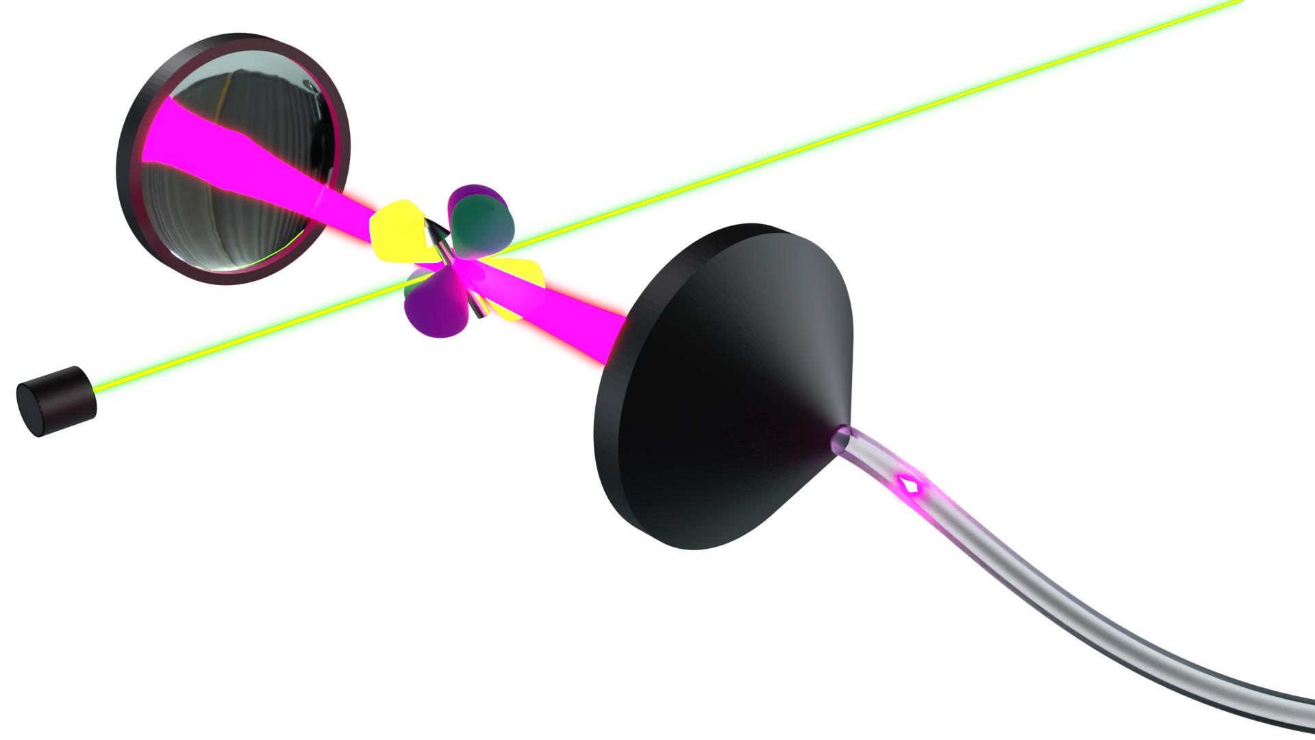
Illustration of a quantum system (silver arrow and yellow, green and purple orbitals) interacting with a resonator (two mirrors and pink light field between them). In addition, the quantum system is controlled by a control field (green laser). A photon (pink luminous drop) has been emitted into an optical fibre through one of the mirrors. Credit & Copyright: Benedikt Tissot
Benedikt Tissot compares the basic procedure with the Internet: “In a classic computer, we have our bits, which are encoded on a chip in the form of electrons. If we want to send information over long distances, the information content of the bits is converted into a light signal that is transmitted through optical fibers.”
The principle of information exchange between qubits in a quantum computer is very similar: “Here, too, we have to convert the information into states that can be easily transmitted – and photons are ideal for this,” explains Tissot.
A Three-Level System for Controlling the Photon
“We need to consider several aspects,” says Tissot: “We want to control the direction in which the information flows – as well as when, how quickly, and where it flows to. That’s why we need a system that allows for a high level of control.”
The researchers’ method makes this control possible by means of resonator-enhanced, stimulated Raman emissions. Behind this term is a three-level system, which leads to a multi-stage procedure. These stages offer the physicists control over the photon that is created. “We have ‘more buttons’ here that we can operate to control the photon,” Tissot illustrates.
Stimulated Raman emission are an established method in physics. However, using them to send qubit states directly is unusual. The new method might make it possible to balance the consequences of environmental perturbations and unwanted side effects of rapid changes in the temporal shape of the light pulse, so that information transport can be implemented more accurately.
The detailed procedure was published in the journal Physical Review Research in February 2024.
Reference: “Efficient high-fidelity flying qubit shaping” by Benedikt Tissot and Guido Burkard, 8 February 2024, Physical Review Research.
DOI: 10.1103/PhysRevResearch.6.013150